Introduction
Among the range of semiconductors, Cadmium Telluride (CdTe) is considered as a promising material in various opto-electronic applications (Duan et al., 2003; Gratzel, 2001; Shaaban et al., 2009). CdTe has also proven to be a good absorber material in thin film photo-device applications due to its ideal band gap near to that of silicon (Rakhshani, 1997). There are many techniques adopted for deposition of CdTe thin films, but vacuum depositions are most preferred due to its flexible and stoichiometric effects (Anthony et al., 1984; Feldman et al., 1981, Al-Ghamdi et al., 2010, Lalitha et al., 2007). The studies on optical, structural, and electrical properties of CdTe thin films have been extensively carried out by several researchers (Khairnar et al., 2003; Youn-Ok Choi et al., 2010; Bacaksiz et al., 2007; Semaltianos et al., 2009), but detailed understanding on optical behavior and characteristics with respect to thickness is sparse, also the accurate measurements of optical like refractive index, extinction coefficient and optical thickness are of great importance, particularly for optical coatings and photo-optical devices.
Numerous methods have been used to understand the thin film thickness and optical parameters. Such methods are classified depending upon the spectra of transmission and reflection, photometric, interferometric, and ellipsometric measurements (Poelman et al., 2003, Nasr et al., 2001, Caliendo et al., 1977). The interferometric and ellipsometric method gives precise measurements, but it requires equipment and experimental proficiency. However, the most simple and widely used technique was the envelope technique which was first given by Swanepoel 1983. By using this technique, the optical parameters can be evaluated from the transmission spectra in strong and weak absorption bands. This technique was recently adopted for amorphous Ge-Se and nano-CdTe thin films on flexible substrates (Pan et al., 2013; Shaaban et al., 2014). The illustration of the envelope method for transmission spectra is as shown in figure 1.
Hence, considering these in this work, we report the systematic investigation on determination of optical parameters and thickness of CdTe thin films by envelope technique and evaluated the thickness dependency on the optical properties of CdTe thin films for photovoltaic device applications.
Experimental
99.99% pure CdTe powder was procured from Sigma Aldrich for deposition of CdTe thin films. The CdTe thin films were prepared over soda lime glass by thermal evaporation technique. The cleaning procedure adopted for substrates was carried out as reported elsewhere (Khairnar et al., 2003). Molybdenum boat was used as sample holder and the separation between the boat and the substrate was kept constant to 13.5 cm. The substrate holder is aided with the continuous rotation for the formation of uniform films. The thin films of 1-4 microns thickness were deposited under the standard rate of deposition (3-5 A°/Sec), which is monitored by in situ digital thickness monitor. The deposited samples were annealed in a vacuum chamber at 350 ºC for 30 min without disturbing the vacuum conditions before and after the deposition processes.
Results and Discussion
- Optical analysis
Figure 2 shows the optical transmittance spectra of 1-4 µm deposited CdTe films in the Vis-NIR wavelength range. For all the film thicknesses, spectral characteristics confirm very significant interference patterns for wavelength next to prominent absorption edge. This tendency of the transmission spectra is a support of the increase in the thickness and uniformity of the films. With the increased thickness, increase in transmittance with sharp shifts in absorption edge in NIR region was evident from the spectra. This behavior could occur due to the increase in absorbance related to changes in surface roughness and this will also have noticeable effects on the propagation of the incident light mainly due to light scattering (Shadia et al., 2013). All the samples revealed more than 60% optical transparency exhibiting increased interference maxima and minima with increasing film thickness in the spectral region between 800 nm to 1100 nm, which in turn gives precise absorption edge reliable to the optical band gap of the thin films. The spectra clearly specify that the transmission is found to decrease with increasing film thickness from 2 µm to 4 µm, which highlight that the CdTe films are having a substantial absorption throughout in the wavelength region 350–800 nm, further the films own weak absorption in the wavelengths above 800 nm.
Fig. 3 represents the normalized transmittance standard deviation with respect to thickness of thin films. The normalized standard deviation showed a minimum value of 0.12% for 2 μm and maximum of 0.32% for 1μm thick CdTe films. As the film thickness is increased from 2-4 μm, from normalized standard deviation it can be inferred that the absorption edge shift becomes less significant compared to 1-2 µm thickness with the average deviation of 0.035%. This deviation drift shows exactly the direct proportion to the flow of the optical transmittance.
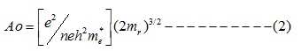
The absorption coefficient can be written as a function of incident photon energy in its broad type is given as (Pankove, 1971),
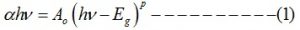
Where ‘p’ has discrete values like 1/2, 3/2, 2 etc. depends on the direct, indirect, allowed or forbidden transitions. In the direct and allowed cases P=1/2 whereas for the direct but forbidden cases it is 3/2. Ao is a constant and it is given by equation (2),
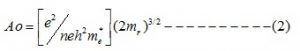
Where and are the effective and reduced masses of charge carriers respectively. Eg is the optical band gap, the value of ‘P’ determines the nature of optical transition.
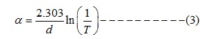
The measured absorbance through spectrophotometer and calculated absorption coefficient are represented in figures 4 and 5 respectively. Using the spectral data the absorption coefficient was calculated using the relation (3),
The maximum optical absorbance for 1 – 2 µm thickness was found to be in the 450 – 550 nm wavelengths, whereas 3 – 4 µm thickness exhibits wide band absorbance from 450 – 700 nm. The mean absorbance of CdTe thin films with different thickness was calculated in the wavelength range from 350 to 1000 nm and is presented in the inset of figure 4.
The mean absorbance increased with thickness and the maximum absorbance revealed for 3 µm thick CdTe. The high absorbance with low value of absorption coefficient exhibited by 3 – 4 µm thin film was due to the increasing recombination of the photo generated electrons under the thickness conditions. The mean absorption coefficient decreases with increase in thickness from 2.07×10⁶ to 6.5×10⁵ for 1 to 4 µm. The reported optoelectronic properties of single crystal CdTe has the absorption coefficient value 6×10⁴ at the wavelength value of 600 nm, which can be achieved with increase in thickness (Mitchell et al., 1977). The 3 µm thick CdTe film exhibits more mean absorption with optimum absorption coefficient compared to rest of the thin films also, the absorption coefficient value confirms that the incident photon of nearly 100% could be absorbed in the visible spectral region with thickness uniformity (Lalitha et al., 2004).
The optical band gap energy of CdTe thin films was estimated from the Tauc plot of (αhν)2 versus photon energy (hν) by a linear extrapolation of each curve to the energy axis in the direct allowed transition as depicted in figure 6. All of the estimated optical band gap energies for various thicknesses are in the range Eg = 1.43–1.50 eV is in good agreement for the single crystal, polycrystalline CdTe thin films (Mitchell, K et al., 1977; Rakhshani, 1997) and also with the earlier reported values (Kim et al., 2010). The inset of figure 6 represents the variation in ln (α) versus photon energy which gives the Urbach tail width, signifies the characteristic phenomena of the absorption curve with respect to photon energy. If the structure of the film has disorderness, we can estimate the level of disorderness using this Urbach energy (Urbach, 1953) which results in lean-in the transmittance spectra towards minimum photon energy. The tail width of the films can be calculated by the slope of the straight line portion of the plot. The optical band gap (Eg) and the tail width (ΔE) of CdTe thin films is shown in table 1.
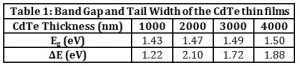
The maximum tail width exhibit by 2 µm CdTe thin film of 2.10 eV, whereas 3 and 4 µm film revealed 1.72 and 1.88 eV respectively. The decreased tail width is the perceptible for the improved grain size of the thin films (Yang Dingyu et al., 2011) which is evident from figure 11.
The refractive index (n) of the film in the medium and weak absorption bands was estimated by using the transmittance maxima and minima as a first approximation according to envelope method. The refractive index was calculated using the equation (4),
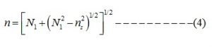
Where,
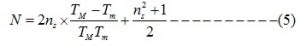
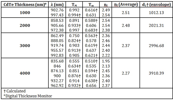
The interference maxima and corresponding minima are represented by TM and Tm respectively. ‘ns’ is the substrate refractive index, which is taken as a standard value of 1.52 for glass. Maxima or minima can be calculated are the transmission maximum and the corresponding minimum at a particular wavelength (λ).
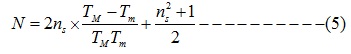
The thickness has been estimated by considering either consecutive maxima’s/minima’s (m = 4) or a maxima and subsequent minima (m = 2) of the envelope at corresponding wavelengths, which is given by,
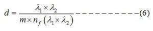
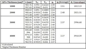
The values of TM, Tm, nf, and d (envelope) is depicted in table 2. The values of refractive index and film thickness are calculated according to the envelope method. The in-situ digital thickness monitor (DTM) was used to cross verify the thickness calculated from the swanepoel method and is confirmed to be a good agreement with the DTM thickness. The average refractive index of the film decreases with increase in thickness and was found to be in the range of 2.51 to 2.27, this decreased trend with respect to thickness can be attributed to increase in absorption and decreased transmission in the weak absorption wavelength.
Table 2: Values of λ, TM, Tm, nf, d(envelope) of CdTe thin films.
The extinction coefficient (k) is a measure of the damping factor of light due to scattering and absorption. It can be determined by using the value of absorption coefficient by using the relation,
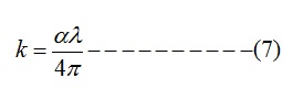
Figure 7 represents the variation of extinction coefficient with respect to wavelength of CdTe thin films. It can be seen that the ‘k’ value decreases with respect to thickness and hence we can say that the loss factor of the incident light has been reduced as the thickness increases. Similar behavior was observed for CdTe thin films deposited on stainless steel substrate (Pantoja et al., 2013).
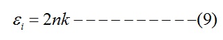
The Loss factor of the thin films shown in figure 8 can be evaluated by real (εr) and imaginary (εi) parts of the complex dielectric constant. The complex dielectric constant is the orientation sum of the dielectric constant and the loss factor components with unity dimensions. The dielectric constants of the CdTe thin films have been evaluated from the following equations (Chambouleyron 2001),
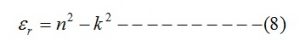
and
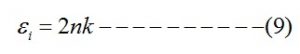
Loss factor,
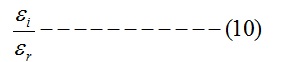
The imaginary part of the dielectric constants in this work decreases with increase in thickness, whereas the real part remains constant with the increase in photon energy. The imaginary part reveals not much variation till 1.45 eV but after that there is a steep increase representing the increased loss. This can be correlated by weak absorption and high absorption coefficient regime. Hence, the photonic loss increases above 750 nm, with a decrease in thickness, which lies in the weak absorption band (Fig. 8).
Figure 9 shows the variation of optical conductivity with the incident photon energy. The optical conductivity was determined using absorption coefficient and the refractive index of the film, which follows the relation (Sharma et al., 2007),
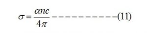
Where, ‘c’ is the speed of light. The steep increase in the optical conductivity from the band edge is due to the high absorbance of CdTe thin films in that region. The decreased optical conductivity with the increase in thickness can be attributed to the decrease in absorption coefficient with an increase in photon energy.
- Structural morphological analysis
X-ray diffraction (XRD) outline for the CdTe thin films, annealed at 350 °C, is shown in Fig.10. There is a single prominent peak at 2θ equal to 24° which correspond to diffraction from the (111) plane of cubic cadmium telluride with zinc blend structure (Jae-Hyeong Lee et al, 2003). The grain size has increased from 54.73 to 59.54 nm for 1 – 3 µm thin films. This shows that the films deposited at a higher thickness has improved grain size. The surface morphology and energy dispersive spectroscopy of 3µm CdTe thin film was shown in Fig. 11.
The film exhibits uniform and compact morphology. The EDAX analysis shows the composition ratios of Cd and Te having 43.6 and 50.7 wt% which reflects that the film posses good stoichiometric values.
Conclusions
The dependency of thickness over optical parameters of vacuum evaporated CdTe thin films was evaluated by envelope technique from the transmittance spectra. The estimated thickness was in good agreement with the in-situ DTM thickness. The determined optical parameters with respect to thickness support the evidence of maximum absorption for 3 µm CdTe thin film with direct allowed transition having optical band gap of 1.49 eV. Grain size evaluated from XRD suggests that it has been increased with increase in thickness with decreased tail width. Also, thin films own good surface morphology and having precise Cd and Te ratios. These are the direct evidence for CdTe thin film which can be used for photovoltaic application.
Acknowledgement
Authors are grateful to CSIR-HRDG, New Delhi, for its financial assistance under the SRF grants No: 09/039(0108)/2013-EMR-I.
(adsbygoogle = window.adsbygoogle || []).push({});
References
- Al-Ghamdi, A, A, Khan, S, A, Nagat, A, and Abdel-Sadek, M. S. (2010) “Synthesis and optical characterization of nanocrystalline CdTe thin films,” Laser Technol., 42(8) 1181-1186.
- Anthony, T, C, Fahrenbruch, A. L, and Bube, R, H. (1984) “Growth of CdTe films by close-spaced vapor transport,” Vac. Sci. Technol., A2 1296-1302.
- Bacaksiz, E, Basol, B. M, Altunbas, M, Novruzov, V, and Yanmaz, E. and Nezir, S. (2007) “Effects of substrate temperature and post-deposition anneal on properties of evaporated cadmium telluride films,” Thin Solid Films, 515(5) 3079-3084.
- Caliendo, C, Verona, E, Saggio, G. (1977) “An integrated optical method for measuring the thickness and refractive index of birefringent thin films,” Thin Solid Films. 292(1-2) 255-259.
- Chambouleyron, I, Martínez, J. M. (2001) “Chapter-12: Optical Properties of Dielectric and semiconductor thin films”. Handbook of Thin Films Materials, edited by H.S. Nalwa Vol. 3, Academic Press.
- Duan, X, Huang, Y, Agarwal, R, and Lieber, C. M. (2003) “Single-nanowire electrically driven lasers,” Nature, 421(6920), 241-245.
- Feldman, B. J, Boone, J. L, and Van Doren, T. V. (1981) “Photoluminescence in spray pyrolyzed CdTe,” Phys. Lett. 38(9) 703-704.
- Gratzel, M. (2001) “Photoelectrochemical Cells,” Nature, 414(6861), 338-44.
- Jae-Hyeong Lee, Dong-Gun Lim, Jun-Sin Yi. (2003) “Electrical and optical properties of CdTe films prepared by vacuum evaporation with close spacing between source and substrate,” Solar Energy Materials & Solar Cells, 75 235–242.
- Khairnar, U, P, Bhavsar, D, S, Vaidya, R, U, and Bhavsar, G. P. (2003) “Optical properties of thermally evaporated cadmium telluride thin films,” Materials Chemistry and Physics, 80 421-421-427.
- Kim, N, H, Choi, Y, O. and Lee, W. S. (2010) “Enhancement of optical properties for CdTe absorber through improving thickness uniformity by CMP process,” Electronic Letters, 46(14) 1019-1021.
- Lalitha, S, Karazhanov, S, Zh, Ravindran, P, Senthilarasu, S, Sathyamoorthy, R, and Janabergenov, J. (2007) “Electronic structure, structural and optical properties of thermally evaporated CdTe thin films,” Physica B, 387(1-2) 227-238.
- Lalitha, S, Sathyamoorthy, R, Senthilarasu, S, Subbarayan, A. and Natarajan, K. (2004) “Characterization of CdTe thin film—dependence of structural and optical properties on temperature and thickness,” Solar Energy Materials & Solar Cells. 82 187–199.
- Mitchell, K, Fahrenbruch, A. and Bube, R. (1977) “Photovoltaic determination of optical absorption coefficient in CdTe,” Appl. Phys. 48 829-830.
- Nasr, A, M, and Sadik, A. M. (2001) “Interferometric studies on thin photoactive polymer films,” Opt. A: Pure Appl. Opt. 3(3) 200.
- Pan, R, K, Tao, H, Z, Wang, J, Z, Wang, J, Y, Chu, H, F, Zhang, T, J, Wang, D, F, and Zhao, X. J. (2013) “Structure and optical properties of amorphous Ge–Se films prepared by pulsed laser deposition,” Optik, 124 4943– 4946.
- Pankove, J. J. (1971) “Optical Processes in Semiconductors,” Prentice-Hall, Englewood Cliffs, NJ.
- Pantoja, J, Enriquez, N, R, Mathews, G, Perez Hernandez, Xavier Mathew. (2013), “Influence of the film thickness on structural and optical properties of CdTe thin films electrodeposited on stainless steel substrates,” Materials Chemistry and Physics, 142(1), 432–437.
- Poelman, D, and Smet, P. F. (2003) “Methods for the determination of the optical constants of thin films from single transmission measurements: a critical review,” Phys. D: Appl. Phys. 36(15) 1850.
- Rakhshani, A. (1997) “Electrodeposited CdTe – optical Properties,” Journal of Applied Physics, 81 7988-7993.
- Semaltianos, N, G, Logothetidis, S, Perrie, W, Romani, S, Potter, R, J, Sharp, M, Dearden, G. and Watkins, K. G. (2009) “CdTe nanoparticles synthesized by laser ablation,” Phys. Lett. 95(3) 033302-3.
- Shaaban, E, R, Yahia, I, S, Afify, N, Salem, G, F, Dobrowolski, W. (2014) “Structural and the optical dispersion parameters of nano-CdTe thin film/flexible substrate,” Material Science in Semiconductor Processing, 19 107-113.
- Shaaban, E. R, Afify, N, and El-Taher, A. (2009) “Effect of film thickness on microstructure parameter and optical constants of CdTe Thin films,” Journal Alloys and Compounds, 482 400-404.
- Sharma, P. and Katyal, S. C. (2007) “Determination of optical parameters of a-(As2Se3)90Ge10 thin film,” Phys. D: Appl. Phys. 40, 2115.
- Swanepoel, R. (1983) “Determination of the thickness and optical constants of amorphous silicon,” Phys. E: Sci. Instrum. 16 1214.
- Urbach, F. (1953) “The long-wavelength edge of photographic sensitivity and of the electronic absorption of solids,” Physical Review. 92(5) 1324.
- Yang Dingyu, Zhu Xinghua, Wei Zhaorong, Yang Weiqing, Li Lezhong, Yang Jun, and Gao Xiuying. (2011) “Structural and optical properties of polycrystalline CdS thin films deposited by electron beam evaporation,” Journal of Semiconductors. 32(2), 023001(1)-023001(4).
- Youn-Ok Choi, Nam-Hoon Kim, Ju-Sun Park, and Woo-Sun Lee. (2010) “Influences of thickness uniformity and surface morphology on the electrical and optical properties of sputtered CdTe thin films for large area II-VI semiconductor heterostructured solar cells,” Material Science and Engineering B, 171 73-78.